
Printed circuit boards are the backbone of virtually every electronic product on the market today. Whether you’re developing an industrial controller, a consumer IoT device, or a medical monitoring system, the quality of your PCB design directly determines whether your product succeeds or fails in the field.
For many companies, especially startups and mid-sized hardware teams, outsourcing PCB design to a specialized service provider makes more sense than building an in-house team. The reasons are straightforward: skilled PCB designers are expensive and hard to hire, design tools like Cadence Allegro or Altium Designer require significant licensing investment, and the learning curve for high-speed or multi-layer designs is steep.
However choosing the wrong PCB design partner can cost you far more than building in-house. Missed DFM rules mean costly board re-spins. Poor signal integrity planning leads to EMC failures. Inadequate documentation hands your CM a puzzle instead of a package.
This guide walks procurement managers and project leads through exactly what to look for when evaluating a PCB design service, so you can make a confident, informed decision the first time.
What Does a PCB Design Service Include?
Before comparing vendors, it helps to understand the full scope of what a professional PCB design service should deliver. Many buyers assume “PCB design” simply means layout, but a complete service covers much more.
- Schematic capture: The design process starts with schematic capture, where the electrical design intent is formalized into a netlist. A good design partner will review your schematic for errors, ambiguities, and component selection issues before a single trace is routed. This stage is where many costly mistakes can be caught for free.
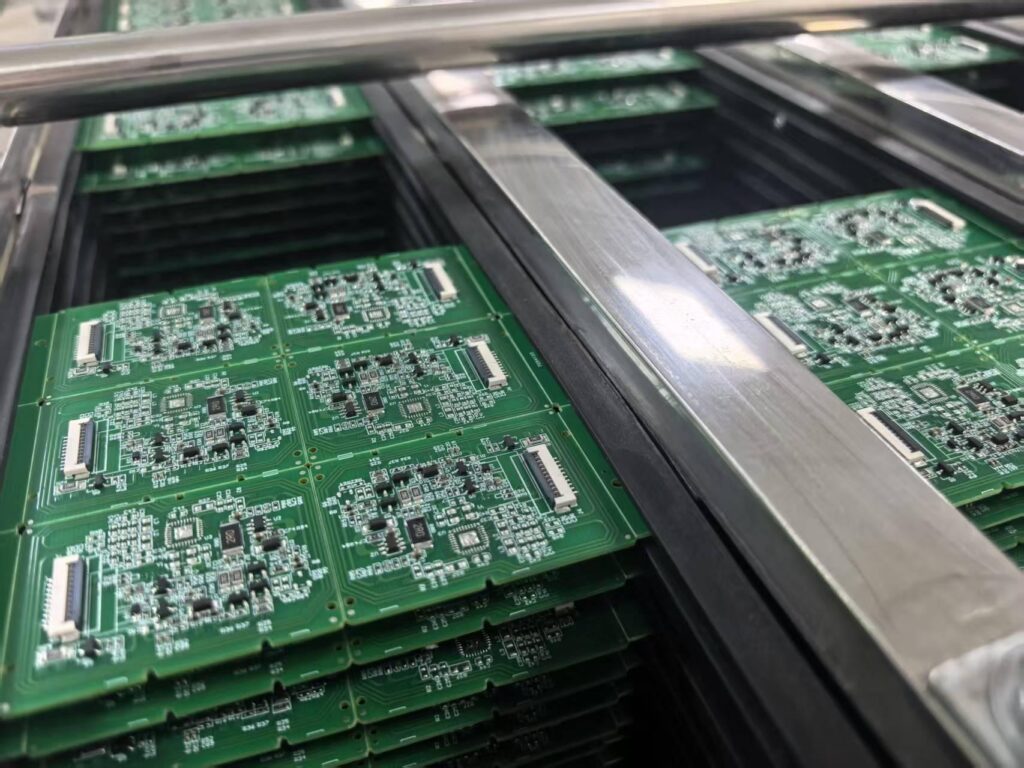
- PCB layout and routing: This is the core deliverable most people think of. It involves placing components on the board and routing copper traces to connect them. The quality here depends heavily on the designer’s experience with your specific design type; a designer experienced in RF layouts may not be the right choice for a high-current power board, and vice versa.
- Layer stack-up design: For multi-layer boards, defining the stack-up is a critical early decision that affects impedance control, signal integrity, EMI performance, and manufacturing cost. A professional service will design the stack-up specifically for your signal frequencies, power requirements, and target fab.
- High-speed design rules: If your design includes DDR memory, USB 3.x, PCIe, HDMI, or any other high-speed interface, your designer must understand controlled impedance routing, differential pair matching, crosstalk mitigation, and return path management. This is a specialized skill, and not every PCB designer has it.
- Design for manufacturability (DFM) review: Before files go to fabrication, a DFM review checks that the design can actually be manufactured reliably. This includes checking minimum trace widths and spacings, via sizes, pad-to-edge clearances, soldermask requirements, and assembly-side component spacing.
- Output files and documentation The final deliverable should include Gerber files, drill files, BOM, assembly drawings, pick-and-place files, and ideally a fabrication notes document. Incomplete output packages are one of the most common sources of manufacturing delays.
5 Key Criteria to Evaluate a PCB Design Partner
With a clear picture of what the service should include, here are the five criteria that matter most when comparing vendors.
- Design capability breadth: Can they handle your specific board type? Ask directly whether they have experience with:
- High-speed digital (DDR4/5, PCIe Gen 3/4, USB 3.x)
- RF and microwave designs
- High-density interconnect (HDI) with microvias
- Rigid-flex and flex designs
- High-current power boards
- A vendor who handles a wide range of design types is more likely to anticipate issues your in-house team might not foresee.
- DFM knowledge and fab relationships: This is arguably the most underrated criterion. A designer who understands manufacturing constraints (and ideally works closely with fabrication partners) will produce designs that go from Gerber to assembled board without surprises. Ask whether they perform DFM reviews internally or rely on the fab to catch issues.
- Communication and project management: PCB design involves dozens of small decisions. Component footprints, via-in-pad choices, connector orientation, test point placement. Each one requires judgment and often a conversation with the client. Evaluate how responsive the team is during the quoting stage. Slow, vague responses at the sales stage usually predict the same behavior during the project.
- Turnaround and revision policy: Understand the expected timeline and how revisions are handled. Most designs require at least one round of client feedback. Is revision time included in the quote?
- How are scope changes priced?
- What happens if the first prototype reveals a design error?
- Is there accountability built into the contract?
- Track record in your industry: PCB design for consumer electronics, automotive, medical, and industrial applications each carry different standards and expectations. A vendor who regularly works in your industry will understand the compliance requirements, reliability expectations, and documentation standards that apply to your product.
Common PCB Design Mistakes and How Professionals Avoid Them
Understanding what can go wrong is useful context when evaluating a vendor’s experience. Here are the most common PCB design mistakes that lead to failed prototypes and expensive re-spins.
- Insufficient ground plane management: Poor ground plane design is one of the leading causes of EMI failures. Many less experienced designers will simply flood ground copper without thinking about returning current paths. A professional understands that high-speed return currents want to travel directly beneath their signal traces, and designs the ground plane accordingly, avoiding splits that force currents to detour and radiate.
- Ignoring thermal relief on power components: High-current components (MOSFETs, inductors, voltage regulators) generate heat that must be conducted away from the board. Insufficient copper pours, missing thermal vias, or poor component placement relative to airflow can cause chronic overheating in the field that doesn’t show up during short-duration bench testing.
- Impedance mismatch on high-speed lines: Unterminated or improperly terminated high-speed lines cause signal reflections that corrupt data. This is especially common on USB, HDMI, and differential clock lines. Proper impedance control requires coordinating trace geometry with the stack-up dielectric properties, which is something that should be calculated, not guessed.
- Antenna effects from floating copper: Isolated copper pours with no connection to ground or power act as antennas, picking up and radiating noise. A professional DFM review always checks for and removes floating copper.
- BOM and footprint mismatches: A component specified in the schematic but without a matching footprint in the layout library causes assembly failures. Professional design services maintain well-managed component libraries and cross-check footprints against manufacturer datasheets before signoff.
The best way to avoid all of these issues is to work with a design partner who has established review checkpoints, and not just a designer who sends you Gerbers when they think it’s done.
High-Speed and Rigid-Flex: When You Need Specialized Expertise
Two design categories deserve special attention because they require skills beyond standard PCB layout: high-speed digital design and rigid-flex design.
- High-speed PCB design: As data rates climb into the multi-gigabit range, PCB design increasingly resembles RF engineering. Trace geometry affects characteristic impedance. Vias introduce stubs that cause resonances. Adjacent traces couple noise into each other. Connector launches must be carefully designed to minimize discontinuities.
If your product includes any of the following, you need a designer with explicit high-speed experience: DDR4 or DDR5 memory, PCIe Gen 3 or higher, USB 3.1/3.2/4.0, 10GbE or faster Ethernet, MIPI interfaces, or high-speed ADC/DAC connections.
Ask prospective vendors to show you examples of successful high-speed designs they’ve completed, and ask whether they performed post-layout simulation or eye diagram analysis to validate signal integrity.
- Rigid-flex PCB design: Rigid-flex boards combine rigid PCB sections with flexible polyimide sections in a single integrated assembly. They’re increasingly common in wearables, medical devices, aerospace systems, and compact industrial equipment where the board must bend or conform to a 3D shape.
Designing rigid-flex correctly requires understanding the mechanical stress on conductors through the flex zone, bend radius constraints, layer transition requirements, and the specific manufacturing capabilities of rigid-flex fabs. It’s a distinct skill set from standard rigid PCB design, and not every PCB designer is qualified to handle it.
For companies that need both capabilities under one roof, working with a full-service provider like TJHXPCB (which offers specialized PCB design services covering everything from standard multi-layer layouts to high-speed and rigid-flex designs), simplifies coordination and reduces the risk of handoff errors between design and fabrication.
How to Brief a PCB Design Firm Effectively
Even the best design partner can only work with the information you give them. A poorly prepared design brief is one of the most common causes of delays, miscommunication, and expensive revisions. Here’s what a complete design brief should include:
- Functional requirements: Describe what the board must do: input voltage range, output requirements, communication interfaces, operating environment (temperature, humidity, vibration), and any relevant standards compliance (CE, FCC, UL, IEC).
- Physical constraints: Board dimensions, connector locations, mounting hole positions, maximum component height on each side, and any keep-out zones should all be specified upfront. If the board fits into an enclosure, share the enclosure CAD model.
- Layer count and stack-up preferences: If you have a preferred layer count or specific impedance requirements, state them. If you’re unsure, ask the vendor to recommend a stack-up based on your signal types and target fab.
- Component preferences: List any preferred component families, existing approved vendor lists, or components you already have in inventory. Specify any components that must be placed in a particular orientation or location.
- Design rule preferences: If your fab has specific capabilities or limitations (minimum trace width, minimum via size, surface finish) include them. If you’re letting the vendor choose the fab, ask them to specify what rules they’ll design to.
- Deliverables and schedule: State the deadline for first layout, the expected review process, and what output files you need. Be specific: Gerber RS-274X, ODB++, IPC-2581, drill files, BOM in specific format, assembly drawings, 3D STEP model.
The more complete your brief, the fewer clarification rounds are needed, and the faster you’ll get a layout you can actually use.
A Checklist for Your Vendor Evaluation
Use this checklist when comparing PCB design service providers:
- ✅ Can they handle your specific board type (standard, high-speed, HDI, rigid-flex)?
- ✅ Do they perform DFM review internally before sending output files?
- ✅ Do they have documented experience in your industry vertical?
- ✅ Is their communication responsive and technically specific during the quote stage?
- ✅ Are revision rounds and scope changes clearly defined in the contract?
- ✅ Can they provide references or example projects similar to yours?
- ✅ Do they coordinate with fabrication and assembly partners, or hand off files blindly?
- ✅ Do they offer full output packages including BOM, assembly drawings, and 3D models?
Choosing a PCB design partner is a risk management decision. The right partner catches problems before they become prototype failures, while the wrong one hands you a set of Gerbers and disappears.
Take the time to evaluate vendors thoroughly, ask the hard questions upfront, and choose a partner whose technical depth matches the complexity of your product. Your next board revision (or the one you avoid entirely) will reflect that decision.